Making a Material Impact
A new Corporate Laboratory has been set up at NUS to research next-generation semiconductor manufacturing processes — essentially doing precision engineering at an atomic level.
POWER PAIRING
Officially launched on 25 October last year, the Applied Materials-NUS Advanced Materials Corporate Lab combines Applied Materials’ expertise in materials engineering and semiconductor technologies with NUS’ multidisciplinary research capabilities that span applied chemistry, materials science and microelectronics process engineering.
Size does matter, though perhaps not in the way most people think. Over the last few decades, computing has become pervasive in everyday life, and this has been possible because computer chips have become more powerful over the years. The increasing power comes from advances in semiconductor manufacturing, specifically the ability to squeeze more and more transistors (which are semiconductor switches) on a computer chip, thus increasing its processing power. Those transistors have been shrinking to the point where Apple’s latest iPhone uses a chip that is made using a 7-nanometre process (a nanometre being a billionth of a metre) with close to 7 billion transistors on a 9mm2 x 9mm2 chip.
“The average size of these miniscule switches is already a thousand times smaller than the cells in our body. By 2020, the number of transistors may be in excess of 12 billion on a 5-nanometre-processed 9mm2 x 9mm2 chip found in our next smartphone,” says Professor Aaron Thean, the co-director of the lab. “The transistor count per chip will far exceed the total human population on Earth.”
The relentless race to the atomic realm drives the global semiconductor industry, which generated more than US$460 billion in revenue last year. In order to steal a march over its competitors, Applied Materials — a leading semiconductor equipment manufacturer — has collaborated with NUS to set up a new corporate lab to develop next-generation semiconductor manufacturing processes that will realise upcoming nanometre-scale technologies. The problems that may arise in these processes will require interdisciplinary expertise, that spans chemistry, material science, and electronic engineering, to solve.
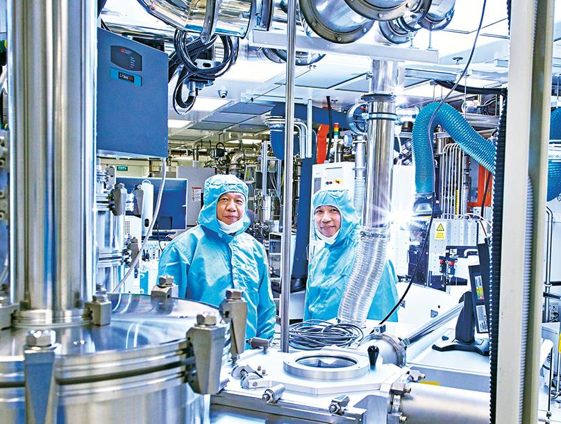 Professor Richard Wong (left) and Professor Aaron Thean in their new state-of-the-art lab.
The Applied Materials-NUS Advanced Materials Corporate Laboratory is one of just five corporate labs in NUS and was launched on 25 October last year. This $70 million facility will tap on the expertise of staff from both the NUS Department of Electrical & Computer Engineering and the NUS Department of Chemistry. According to Prof Thean, the collaboration came about because Applied Materials was looking for a university to do “out-of-the-box innovation,” to find completely new ways to engineer material starting from the very fundamentals of chemistry — and NUS embodies all those capabilities. The lab will leverage on NUS’ scientific knowledge in advanced materials built up over more than 20 years. Because the scale of manufacturing these chips is now at the deep-nanometre level, the lab will be doing “precision engineering at the atomic scale”, as Prof Thean describes it. Prof Thean, a prolific inventor with more than 50 US patents in advanced electronics, is the Director of NUS’ new Nanofabrication Facility, E6Nanofab.
“NANO”-MANAGEMENT 101
Working at the atomic level has numerous challenges. Among other things, materials behave differently when they are this size. In addition, the materials are so small that their surfaces and interfaces must be carefully engineered for the best performance. In addition, multiple thin nano-scale materials are being stacked together so that they can work as a single entity. All this requires fundamental understanding and innovative research into new materials and their behaviour at an atomic level. If successful, these research projects will lead to smaller and more power-efficient transistors — and thus more powerful computer chips. This can translate to greater storage capacity for USB drives, and faster chips in smartphones, laptops and servers. It will also lead to more computing power to handle the needs of processor-intensive applications like artificial intelligence and storage, processing and analytics.
One of the projects, for example, is looking at a completely new way of etching a semiconductor wafer. Etching is the process during semiconductor manufacturing which uses chemicals to remove layers from the surface of the wafer. As part of this process, some areas have to be masked off so that the unwanted exposed layers can be removed. Currently, etching is done using a process known as photoresist but the new lab is looking at using an atomic layer of carbon to mask areas instead. This would result in a much thinner mask than the current process. “The lab is looking at the ability to deposit the carbon layer as a mask reliably and accurately,” says Prof Thean.
Another research project is looking at improving the wafer fabrication process by using graphene, a type of carbon that is ultra-strong, as a diffusion barrier. In computer chips, barriers are needed to chemically isolate semiconductors from the soft metals used to electrically interconnect them. In a modern computer chip, for example, all the copper used to conduct electricity must be surrounded by a barrier to prevent the copper from diffusing into the surrounding materials. Currently, tantalum nitride, an inorganic chemical compound, is used as the barrier. Graphene, which consists of a single layer of carbon atoms, would result in a much thinner, stronger barrier. “Ultimately, to build the next big technology we will start from the tiniest of parts, and this requires us to innovate at the atomic level for industrial scale,” adds Prof Thean.
A MEETING OF MINDS
According to Professor Richard Wong, the Head of NUS Department of Chemistry and a co-director of the lab, the departments will be looking at developing ways to create the new processes needed to work at the atomic level. The project looking at graphene as a barrier, for example, will call on the expertise of groups in the Chemistry department in graphene chemistry, says Prof Wong, who was awarded the 2018 Fukui Medal in recognition for his outstanding contributions to the application of computational chemistry to physical organic chemistry.
About 30 people have been hired for these projects so far, and the lab hopes to eventually hire 50 engineers, researchers and post-doctorates. According to Prof Thean, ideas are already being generated now that will lead to patents. The hope is that in five to 10 years’ time, the lab will be able to develop new processes that Applied Materials can commercialise and use. Speaking at the official launch of the lab on
25 October 2018, Finance Minister Mr Heng Swee Keat noted that the lab will also “reinforce NUS’ efforts
in building research capabilities to ride the new waves of technological shifts in artificial intelligence, semiconductor technology and the Internet of Things, which can then be applied in areas like autonomous vehicles, robotics and many others.” The research being done in the lab also fits into Singapore’s economic strategy, as electronics is a key part of Singapore’s manufacturing sector. Singapore is among the top locations in the world for advanced semiconductor manufacturing, Mr Heng pointed out, and currently,
more than half of the world’s semiconductor companies do research and development, as well as manufacturing here.
Text by Jimmy Yap
*Source: businesstimes.com.sg